
This is going to be a very, very long post, guys. So please, grab a cup of coffee, put on some sweet music, and read on...
In this first issue of TechTalk, we will provide you with a basic understanding on how a CPU works, how this is then crammed into our smartphones, and we'll finish looking at the most common CPU running on many devices being sold today. Tech lovers, gadget lovers, computer software architecture students, this post is for you!
Introduction to Basic CPU Architecture

CPUs, in the beginning, used to store numbers like we do, in the decimal numeral system. However, this proved to be very inefficient compared to storing numbers in the binary numeral system, where every digit can only have a value of 0 or 1, and where digits are called bits. Thus, numbers are stored in bit arrays of a certain width or length n, where the smallest number we can store is zero, and the biggest 2^n. These bit arrays, are called registers.

A typical CPU will have a few internal registers, and at least two interfaces with other chips, the memory bus and the data bus. Buses are like channels through which bits can flow, and have a certain width; a 16 bit wide bus can only transfer (or hold) one 16 bit number at a time.

In computer architecture, a 32-bit CPU is a microprocessor in which all of its registers are at least 32 bits wide, and both the data bus and memory bus are also at least 32 bits wide; if, for example, a CPU has 32 bit registers, a 32 bit memory bus and a 64 bit data bus, it is still considered a 32 bit microprocessor, because its "native" data unit is a 32 bit number; all the registers and the memory bus would have to be 64 bits wide for the CPU to be considered a 64 bit microprocessor. The architecture also limits the number of instructions, or operations the CPU understands, and the amount of memory blocks (which are the size of the internal registers) it can access; this number is very big for the number of instructions, so it doesn't represent a limitation here, but it does for the amount of memory; a 16 bit CPU can only have access to (or address) 64 KiloBytes (2^16 blocks) of memory and a 32 bit CPU as much as 4 GigaBytes (2^32 blocks).
All of the programs a CPU runs, are made up of a sequence of instructions. All CPUs have their own "set" of instructions, also called Instruction Set Architecture (ISA), or Computer Architecture; the most famous computer architecture is Intel's x86 architecture. Since CPUs of the same architecture share the same instruction set, they will run exactly the same software. CPUs which are part of an architecture evolve over time; for example, the Intel 8086/8088 had a certain set of instructions, and the following Intel 286 understood the same set of instructions plus new ones which enabled the new chip's features. Internally, at a circuitry level, the CPUs might not be the same, but a program designed and built for a 8086/8086 would run perfectly on a 286 and subsequent versions, because the same sequence of instructions is still performed with the same results. This, for example, allows us to run a version of Microsoft Windows designed for the Intel Pentium CPUs in more modern Intel Core 2s or Intel Core i7s.
Now, we need to dig a bit deeper. As we just mentioned, programs are a sequence of instructions performed or executed by the CPU; for the CPU to execute a single instruction, it must perform a series of operations, called the instruction cycle; this instruction cycle is repeated again and again, millions and millions of times, from the second we turn on our system, until the second we turn it off. These instructions are stored in memory, so the CPU needs to perform a request to memory for each instruction; as incredible as it sounds, data for our programs is also stored in memory, because the CPU needs its registers to perform the instructions.

As you can see, the instruction cycle takes 5 steps, which we call stages. On the first stage, the instruction to be executed is requested by the CPU to memory; this is done thanks to a special register, called Program Counter (PC) which holds the address in memory of the next instruction. Once the CPU gets the instruction, it stores it in another special register called Instruction Register (IR); in the decode stage, the CPU must "break" the instruction and understand which operation must be performed. In the next stage, the CPU looks for the operands and prepares for the execution stage; for example, in an add instruction, one operand might be in memory while the other one might be stored in a register inside the microprocessor. Then, the instruction is performed (executed), and finally, in the retire stage, the results are stored in a register or in memory, and the PC is incremented so that it holds the address for the next instruction. The process is beautifully represented here by tech master Anand Shimpi (I simply changed the background):


As you can see, when a stage is completed, it is filled with a completely different instruction; this is called a pipelined microprocessor, and it provides us with an important performance boost, but, at a cost.
First, let's study the effect of the pipeline. We have 5 stages, meaning if our CPU wasn't pipelined, the amount of time necessary to execute a single instruction would be the total time the instruction spends in all of the stages. Supposing all stages take 1ns, except the decode stage which takes 3 ns, our CPU clock must be set at 3ns (the slowest stage's time), meaning our speed will not be faster than 1/3ns = 33 Mhz but, 33 Mhz does not mean 33 million instructions per second (MIPS), it means 33 million clock cycles per second, and because it takes us 5 clock cycles to perform a full instruction cycle, we're actually looking at no more than 7 MIPS. With a pipeline, however, we get the benefit of finishing an instruction every clock cycle, as long as our pipeline is full, which takes us 5 clock cycles to do. So with a pipelined CPU, we are looking at around 33 MIPS.
The drawback? Many times, our computer programs do not execute the next instruction in the IR; maybe the instruction currently in the execution stage changes the address of the next instruction (which happens in a loop), meaning our pipeline has to be completely washed out and filled again, because the instructions in the previous stages are not the next ones we need to execute. This problem is partially solved by many processors with a branch predictor; a dedicated part of the CPU which tries to anticipate which will be the next executed instruction, in order to prevent this situation from happening as much as possible.
Now, say that we want to improve our CPU's performance; the first thing we see is that our decoding stage makes us slow. Supposing all of our stages took 1ns to complete, our clock cycle could be set to 1ns, meaning 1/1ns or 100Mhz, but how? Making the pipeline deeper; by breaking the single decode stage into three separate ones, each taking 1 ns, we get 8 stages, all with a 1ns time.

Is there a new drawback? Yes, there always is; if we need to wipe our pipeline because we failed to predict the next instruction, it now takes us as much as 8 clock cycles to reach our peak performance of 100Mhz (100 MIPS), and in the meantime, there are no instructions leaving the pipeline; we're performing at 0 instructions per clock cycle, which is not good. There are also certain situations in which a certain stage will take more time, and "stall" the whole pipeline, which would greatly affect our performance, since all instructions in the previous stages must wait for the stalled stage to finish in order to continue; this is called in-order execution.
Finally, to finish our visit through CPU Architecture, we'll take a glance at how the CPU is connected to other elements in a standard PC (the Core i3s, i5s, i7s and i9s do not meet this since Intel's revised the architecture):
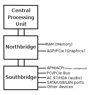
The Northbridge is where the CPU connects with the most important chips it needs to work with; the connection between the CPU and the Northbridge is done by the Front Side Bus (FSB), and through this bus, the CPU has access to the memory and the Graphics Processor Unit (GPU), which are directly connected to the Northbridge. In the Southbridge, we have very slow chips (in comparison to the CPU, Memory and GPU), like Hard Drives, Ethernet, Sound, Printers, etc. which are typically known as Input/Output (I/O) elements.
Into ARM territory
At last, we arrive at smartphone territory. Before starting to build our smartphone though, we must review one last concept: the CPU's fabrication or manufacturing technology. It so happens that there's a law, called Moore's Law, which states that every two years, CPUs double their performance; it's actually more complicated, but this is the basic idea. Now, how is this possible? Well, it has been possible, because CPUs have become smaller and smaller, and keep getting smaller in such a way that we can make twice as complex CPUs (and thus, twice as fast) using the same space (size) we needed two years ago. This, of course, is no where near easy to do, and the tech industry spends millions and millions of dollars in R&D to achieve this, but it keeps on happening, more or less at the same rate.
A very important factor in this war (size vs. performance) is the fabrication process; the smaller the fabrication process, smaller the CPU; so if we build two CPUs, using exactly the same design, one with a 130 nm (nanometers) and other one with a 90 nm process, the second one would be around 30% smaller physically. So, the smaller the fabrication process, the better. This is also important for power consumption, since smaller CPUs require lower power, and produce less heat.
Now, let's talk about our business. The CPU industry around smartphones and similar systems (called embedded systems) works very differently to the PC market, where Intel, AMD, Nvidia and others make their own CPU designs, and build them themselves. In the world of embedded systems (which includes smartphones), the story is quite different, and like in the PC market everything spins around Intel and Nvidia, in the smartphone market, it's around ARM and PowerVR.
We're not here to discuss smartphone GPUs, so we'll leave PowerVR aside for now, and focus on ARM.

In the embedded systems market, ARM makes the design for the CPUs, and these designs are then licensed by manufacturers like Qualcomm, Samsung, Marvell, Nvidia, Texas Instruments, etc. and built by them. Many manufacturers make their own changes, but the CPUs still meet the ARM architecture specifications. It is important to note that ARM designs the CPU and its interfaces to other components, but nothing else; it is up to manufacturers to build the physical CPU, connect it to memory, GPU, the telephony radios (GSM, GPRS; EDGE, 3G, CDMA,...), Wi-Fi chip, and all of the other components. In other words, ARM designs the CPU and the connections to the Northbridge, while the manufacturer actually builds the CPU, the Northbridge and the Southbridge.
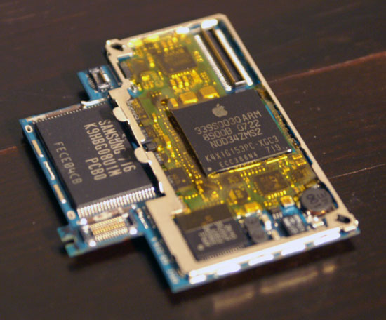
Because smartphones need to be so small, so light, and so fast, the architecture and the interfaces are radically different; all of the components are massively crammed together; in fact, all of them (memory, GPU, Wi-Fi, GPS, telephony radios, accelerometer, digital compass, etc.) are built into a single chip, called a SoC or System-on-a-chip. To aid the ARM core from having to take on all of the tasks, it is supported in the SoC by other cores called DSPs or Digital Signal Processors, which relieve the ARM core from many tasks like processing the signal from the smartphone's camera, the microphone, handling the telephony radios, etc. Manufacturers brand their SoCs based on an ARM CPU as platforms, and offer a range of chips with different performance within the same platform; for example, many Android smartphones use a Qualcomm MSM platform to run, the most widely used being the ARM11 based MSM7200A model. (Picture of the iPhone 3G SoC built by Samsung below)
This strategy of separating design from manufacturing has proven to be very successful for the embedded systems market; on the one hand, ARM knows how to design chips, and does not need to spend the money to build them, while on the other hand, manufacturers know how to manufacture and "pack" CPUs into SoCs, and with a license, they avoid all the costs of designing their own CPU architecture, and even get to make small changes of their own. The fact that all smartphones use ARM based CPUs opens the door for porting the mobile Operating Systems between devices, since these CPUs use the same instruction set and theoretically, all of them can run the same Operating Systems. In practice, however, this is not so easy, because smartphones have hundreds of different chips crammed into the SoC, and a small program called driver is required by the Operating System to "know" how to use each SoC component, so it takes skill and time to perform these "hacks" (hats off to all smartphone hackers!).
Now, the ARM CPU which runs under the hood of many of our smartphones.

Currently, the most used version of the ARM architecture is the ARM11. The ARM11 was first released on 2002, and its latest version, on 2003; however, it wasn't used in a smartphone until 2007. This is a common practice with ARM designs, like with the new generation ARM Cortex A8, which was released on 2005, but wasn't actually used on a smartphone until last year.
The ARM11 is a 32 bit 8 staged pipelined microprocessor, typically built with a 90 nm manufacturing process, using the ARMv6 instruction set, featuring instructions specially designed to accelerate audio and video applications; it improves the interface for sharing information with other chips in the SoC compared to its predecessor, the ARM9, a much more advanced branch predictor capable of "remembering" branches for a short time to improve performance, and is capable of running memory-related instructions and arithmetic/logic instructions at the same time in the final stages of the pipeline. In performance terms, the first versions of the ARM11 core ran between 200 and 500 Mhz, but the 1 Ghz mark is achievable, according to the official documentation. Smartphones using ARM11 cores include both the iPhone and the iPhone 3G (1G and 2G iPod Touch too), Android devices like the HTC Dream/G1, HTC Magic/G2, HTC Hero, HTC Tattoo, Samsung Galaxy, Motorola Cliq, Nokias like the E71, 5800 XpressMusic, N95, N97, and many others.
The ARM11 was a great step forward, considering its design was released in 2003, specifically designed for smartphones, which at that time, where not a part of mainstream consumers' knowledge. However, it's grown terribly old now, and its performance is no where near what's required in today's mobile platforms, but don't worry, ARM has came to the rescue, and we'll study the new ARM architecture in our next issue of TechTalk. Thanks for reading!
Special Thanks To:
Anand Shimpi, from AnandTech.com, for his amazing post "Understanding the iPhone 3GS", which inspired this column, and my computer hardware architecture professors at Universidad de La Laguna, Spain, for making me understand how instructions come to life inside a microprocessor.
References:
http://en.wikipedia.org/wiki/System-on-a-chip
http://en.wikipedia.org/wiki/Transistor
http://en.wikipedia.org/wiki/Moore%27s_Lawa
http://en.wikipedia.org/wiki/Semiconductor_manufacturing
http://en.wikipedia.org/wiki/Northbridge_%28computing%29
http://en.wikipedia.org/wiki/Instruction_set
http://en.wikipedia.org/wiki/Integrated_circuit
http://en.wikipedia.org/wiki/Central_processing_unit
http://en.wikipedia.org/wiki/ARM_architecture
http://en.wikipedia.org/wiki/ARM11http://www.engadget.com/2009/10/14/core-values-the-silicon-behind-android/
http://www.anandtech.com/gadgets/showdoc.aspx?i=3579
http://www.anandtech.com/gadgets/showdoc.aspx?i=3595&p=2
http://www.anandtech.com/gadgets/showdoc.aspx?i=3595&p=4
http://www.cs.uiuc.edu/class/fa05/cs433ug/PROCESSORS/ARM%2011%20MicroArchitecture.pdf


1 comment:
I am planning to write a white paper on how to clock different components in the SOC using external clock chip from Spectralinear www.spectralinear.com
Post a Comment